ClassOne Technology Receives Order for Solstice® S8 Single-Wafer System from Finland’s VTT Technical Research Centre

Prominent European research institution to leverage Solstice platform’s leading-edge electroplating technology for advanced packaging applications
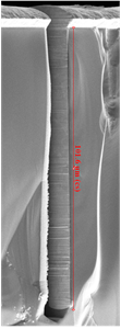
VTT Technology Research Centre to use ClassOne Solstice S8 for advanced packaging
KALISPELL, Mont., Nov. 09, 2023 (GLOBE NEWSWIRE) -- ClassOne Technology, a leading global provider of advanced electroplating and wet processing tools for microelectronics manufacturing, today announced that leading European research institution VTT Technical Research Centre of Finland has placed its first order for a ClassOne Solstice® S8 single-wafer system. VTT will leverage the tool’s production-proven electroplating capabilities to perform advanced through-silicon via (TSV) processes for a range of applications, from MEMS packaging to 3D integration of novel sensor chips and quantum computing.
According to industry research firm Yole Group, the advanced packaging (AP) sector is expected to realize a compound annual growth rate of 10% between 2022 and 2028, exceeding US$78 billion by 2028. Primary market drivers are shifting, as mobile and consumer decrease share while automotive and telecoms gain. Dominant packaging technologies flip-chip, 2.5D/3D and system-in-package (SiP) are expected to represent 90% of the AP market by 2028.
VTT will use the Solstice system to add new copper TSV capabilities, enabling utilization of advanced electrolyte chemistries, and atomic layer deposition (ALD) seed layers for bottom-up TSV plating. “VTT has traditionally been focused on high-density bumps for detectors and basic packaging applications. As we turn our efforts toward advanced packaging, we seek to develop contemporary solutions for critical TSV and damascene processes,” said James Dekker, senior MEMS research scientist with VTT. “The Solstice system from ClassOne is vital to our work in these applications, which have been heretofore impossible to approach reliably.”
The Solstice single-wafer platform can combine multiple process technologies and chemistries in a single, small-footprint configuration for advanced chip packaging applications. VTT’s Solstice S8 system chambers will include Vacuum Prewet for high-aspect-ratio features; CopperMax™ and Copper Gen4 ECD for plating; and spin-rinse-dry (SRD) for clean, fast wafer drying post-plating.
Noted ClassOne Technology CEO Byron Exarcos, “We welcome VTT as a new customer for our Solstice platform. We’re seeing heightened interest in advanced packaging technologies from institutions and universities, and Solstice is perfectly poised to help them make the leap to single-wafer from batch processing. The work that VTT and other organizations are pursuing is vital to developing new capabilities that will impact the future of microelectronics manufacturing.”
The Solstice platform’s flexible operation combines automation with manual operation, making the tool attractive for both R&D and pilot-line use, both of which VTT will use the tool to pursue. In addition, the firm plans to provide access to the tool for qualified customers needing Solstice’s unmatched capabilities to help advance their production efforts. ClassOne will ship the Solstice S8 to VTT’s head facility in Espoo, Finland.
ClassOne will be exhibiting next week in booth B1441 at SEMICON Europa, running from November 14-17 in Munich. Please visit us to learn more about our Solstice single-wafer platform as well as our Trident™ batch processing systems.
About ClassOne Technology
ClassOne Technology is a leading provider of advanced electroplating and wet processing systems for semiconductor and microelectronic device manufacturing around the world. Its advanced IP portfolio comprises highly customized, cost-effective processing solutions for critical wafer processes used to manufacture compound semiconductor devices for photonics, power, 5G, microLED, and MEMS and sensor markets. With tools installed in leading-edge fabs and research organizations worldwide, ClassOne’s flagship Solstice platform is highly configurable, comprising fully and semi-automated electroplating and wet processing applications with the industry’s most competitive ROI. For more information, please visit classone.com. Stay in touch with us: LinkedIn | Twitter
For more information, contact:
Sales Inquiries | Media Inquiries |
Byron Exarcos | Angel Jansky |
ClassOne Technology | Kiterocket |
tel: +1 678.772.9086 | tel: +1 909.224.6273 |
email: pr@classone.com | email: ajansky@kiterocket.com |
|
|
Solstice is a registered trademark and Trident is a trademark of ClassOne Technology.
A photo accompanying this announcement is available at https://www.globenewswire.com/NewsRoom/AttachmentNg/3df60d7a-8450-42e5-936f-9e100d2fbde3

